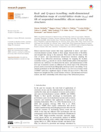
Real- and Q-space travelling: multi-dimensional distribution maps of crystal-lattice strain (∊044) and tilt of suspended monolithic silicon nanowire structures
- Dolabella, Simone EMPA, Swiss Federal Laboratories for Materials Science and Technology, Center for X-ray Analytics, Dübendorf, Switzerland - Department of Chemistry, University of Fribourg, Switzerland
- Frison, Ruggero EMPA, Swiss Federal Laboratories for Materials Science and Technology, Center for X-ray Analytics, Dübendorf, Switzerland
- Chahine, Gilbert A. ID01, European Synchrotron Radiation Facility (ESRF), Grenoble, France - Université Grenoble Alpes, CNRS, Grenoble INP, SIMAP 38000, France
- Richter, Carsten ID01, European Synchrotron Radiation Facility (ESRF), Grenoble, France
- Schulli, Tobias U. ID01, European Synchrotron Radiation Facility (ESRF), Grenoble, France
- Tasdemir, Zuhal Department of Mechanical Engineering, Koc University, Sariyer, Istanbul, Turkey
- Alaca, B. Erdem Department of Mechanical Engineering, Koc University, Sariyer, Istanbul, Turkey - Surface Science and Technology Center (KUYTAM), Koc University, Sariyer, Istanbul Turkey
- Leblebic, Yusuf ARTORG Center for Biomedical Engineering Research, University of Bern, Switzerland - École Polytechnique Fédérale de Lausanne, (EPFL), Lausanne, Switzerland - Sabanci University, Istanbul, Turkey
- Dommann, Alex EMPA, Swiss Federal Laboratories for Materials Science and Technology, Center for X-ray Analytics, Dübendorf, Switzerland - ARTORG Center for Biomedical Engineering Research, University of Bern, Switzerland
- Neels, Antonia EMPA, Swiss Federal Laboratories for Materials Science and Technology, Center for X-ray Analytics, Dübendorf, Switzerland - Department of Chemistry, University of Fribourg, Switzerland
-
01.02.2020
Published in:
- Journal of Applied Crystallography. - 2020, vol. 53, no. 1, p. 58–68
English
Silicon nanowire-based sensors find many applications in micro- and nano- electromechanical systems, thanks to their unique characteristics of flexibility and strength that emerge at the nanoscale. This work is the first study of this class of micro- and nano-fabricated silicon-based structures adopting the scanning X-ray diffraction microscopy technique for mapping the in-plane crystalline strain ([epsilon]044) and tilt of a device which includes pillars with suspended nanowires on a substrate. It is shown how the micro- and nanostructures of this new type of nanowire system are influenced by critical steps of the fabrication process, such as electron-beam lithography and deep reactive ion etching. X-ray analysis performed on the 044 reflection shows a very low level of lattice strain (< 0.00025 Δd/d) but a significant degree of lattice tilt (up to 0.214°). This work imparts new insights into the crystal structure of micro- and nanomaterial-based sensors, and their relationship with critical steps of the fabrication process.
- Faculty
- Faculté des sciences et de médecine
- Department
- Département de Chimie
- Language
-
- English
- Classification
- Chemistry
- License
-
License undefined
- Identifiers
-
- RERO DOC 328183
- DOI 10.1107/S1600576719015504
- Persistent URL
- https://folia.unifr.ch/unifr/documents/308616
Other files
Export to…
Statistics
Document views: 219
File downloads:
- pdf: 264
- Supplementary material: 232